This badge is designed to highlight digital fabrication techniques that are commonly used in the Neurotechnology Core(NTCore) at the Center for Brain Science at Harvard University.
The NTCore works to accelerate and advance scientific progress through:
- design and fabrication of novel instrumentation
- user training and access to a shared fabrication space
- consultation on instrumentation use, design, fabrication, and purchase
By building a badge users will learn about:
- electronics design including making a custom printed circuit board (PCB) using the free and open source KiCad design software
- electronics fabrication including soldering of surface mount electronics
- embedded programming using the Arduino environment
- designing mechanical parts using Autodesk Fusion360 (free to academics)
- digital fabrication using 3D printing and laser cutting for rapid prototyping and production
We are happy to offer customized assistance. For the badge you can choose to:
- Assemble pre-built parts
- Build (by soldering, laser cutting, etc...) and then assemble parts
- Design your own parts (we're happy to help!)
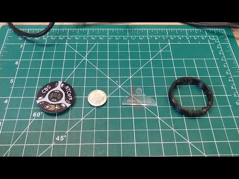
Your badge comes in 4 major parts and requires some minor assembly before use:
- Electronics
- Battery (CR2032)
- Laser cut case back cover
- 3D printed case
Below is a description of the assembly steps followed by a video of the assembly process.
- Install the battery into the electronics (positive side out).
- Insert the electronics into the case from the back making sure that the electronics slide behind the 6 plastic tabs.
- Slide the laser cut case back cover in place to lock the electronics into the case.
- Test the badge by pressing your finger against the two neurons at the bottom of the badge. If your hands are very dry you may need to slightly moisten your finger before touching the badge.
Click the image below for a short (~1 min) video showing the assembly process.
The hole at the top of the laser cut piece can be used to hang the badge from a lanyard, carabiner or cord.
If you are interested in more building experience, follow along with building the parts of the badge.
Badge building involves 5 steps:
- soldering electronic components to the badge printed circuit board
- programming the microcontroller
- 3D printing the main case body
- laser cutting a custom case back cover
- assembling your badge
![]()
Although it is possible to fabricate your own printed circuit boards, the results are often less precise and more time consuming than ordering a custom board. The cost of the board will depend on the difficulty in fabricating the design, the lead time for the order and the quantity ordered. Designs that have traces (wires embedded in the PCB) that are less than 6 mils (thousandths of an inch) or have many layers (pcbs are made by stacking layers of fiberglass, patterned copper and other materials) are typically manufacturable at an increased cost or lead time. The design for this badge is relatively simple and can be made by most low cost venders ('fab houses') including OSHPark. OSHPark is highly recommended as they produce high quality boards with a relatively short lead time (typically a week) at a USA location allowing for overnight shipping. For their 'Prototype' service they charge $5 per square inch for a 2 layer PCB. The badge is 2.25 square inches costing $11.25 per board. When ordered with their 'Medium Run' bulk service (which requires ordering at least 100 square inches) the cost drops to $2.25 per board.
![]()
KiCad is a free and open source electronics design program that runs on all modern operating systems. It's design process involves a number of steps often starting with making a schematic of the circuit you would like to build. This schematic typically includes several components (including resistors, capacitors, connectors, integrated circuits etc) connected using traces (wires embedded in the final PCB design). After a schematic is drawn some automated tests should be run (electrical rules check or ERC) to check for incorrect or missing connections. The final schematic and components can then be exported as a 'netlist', footprints (custom copper shapes that fit specific components) can then be associated with the netlist components and then imported into the pcb layout editor. In the pcb layout editor footprints are placed on a layered design (typical low cost boards have 2 copper layers 'top' and 'bottom') and traces are drawn to connect footprints based on the connectivity defined in the netlist. Before finalizing a design the pcb layout editor can run several automated checks (design rule checks or DRC) to verify that your design matches the capabilities of the fab house (you will need to input these design rules into the editor). Fab houses typically accept gerber files (a special file format that contains images of layers of the pcb and other features needed for fabrication). However, some houses including OSHPark will directly accept KiCad designs.
![]()
If you have not soldered before, adafruit.com has a very good guide to soldering including tips on surface mount soldering.
All the electronic components are surface mount devices (SMD) which attach to copper 'footprints' on the top or bottom of the badge.
It's often helpful to start with the shortest parts and solder the largest parts last (connectors and in this case the battery tab). For this badge you might want to solder parts in the following order:
- ATTiny (U1): the black 8 pin chip that goes in the middle
- Capacitor (C1): the small tan colored device
- Resistors (R1-R4): a 106 (10 MOhm) resistor (R4) and 3 x 471 (470 Ohm) resistors one for each LED (R1-3)
- LEDs (D1-3): light emitting diodes, clear side up, green arrow down
- battery holder (on back): make sure the battery slides in from the edge of the badge
![]()
Some parts (the LEDs and ATTiny) only work when connected in one orientation. Be sure to connect:
- the pin on the ATTiny next to the dot to the pad marked with an extended line
- the green marked ends of the LEDs with the closed end of the lines
Soldering SMD electronics takes some practice and a few tips can make the process much easier. One useful technique is to solder 1 pin at the corner of a part. This pin can be reheated and the part position adjusted with forceps while the solder is molten. When the part is correctly aligned the opposite pin can be soldered to lock the part in place before soldering the remaining pins.
It's time to solder the components on the front of the badge:
- U1: black 8 pin ATTiny, note the orientation
- C1: tan capacitor
- R4: 106 (10 MOhm) resistor
- R1: 471 (470 Ohm) resistor
- R2: 471 (470 Ohm) resistor
- R3: 471 (470 Ohm) resistor
- D1: LED, note the orientation
- D2: LED, note the orientation
- D3: LED, note the orientation
Finally, flip over the badge to prepare to solder on the battery clip.
![]()
Solder the back battery holder taking care as the iron will quickly heat up the entire metal clip. Allow the clip to cool down between applications of heat while adjusting the clip. Be sure to add plenty of solder to create a solid connection that will resist the spring force of the clip when the battery is inserted.
The badge contains a microcontroller, a small computer designed to produce and sample digital and analog signals. The microcontroller can be programmed (more on this below) to produce precisely timed pulses, read and record analog voltages, control other electronics (lights, sensors, motors, etc), perform complicated logic (state machines, event loops) and many other tasks. Many types of microcontrollers are available with different amounts of processing power, number of connections and specialized hardware (including wifi and other wireless communication). The badge circuit uses a simple and low cost ATTiny. This ATTiny has only 8 connections (pins) and requires only a program and a connection to power and ground to function. For the badge 3 pins are connected to light emitting diodes (LEDs) and one more pin is connected to a custom neuron footprint used as a touch sensor.
Arduino is a beginner friendly environment for writing programs for and configuring microcontrollers. There are many official and non-official 'Arduino compatible' boards which can be programmed with the Arduino integrated development environment (IDE). Arduino programs are written in the C++ programming language and use functions that simplify the process of setting or reading the state of digital and analog pins and other aspects of using a microcontroller. Development using Arduino starts with installing the IDE, adding support for the board you'd like the use, installing any required libraries, and then writing your program and 'uploading' it to your board. Most boards can be programmed over USB. However, the badge uses a simpler method called 'in circuit serial programming' (ICSP) that requires a custom programmer (such as the Pocket AVR Programmer or USBtinyISP). To compile code for the ATTiny you will need to install support for the ATTiny from here: https://github.com/damellis/attiny
For a detailed course on using Arduino please see the 'Arduino for Biologists' nanocourse.
![]()
The badge 'firmware' (software for embedded hardware) simulates 3 neurons connected in a ring with 3 model excitatory synapses. The spike output of each neuron is mapped to a different LED which flashes when the neuron spikes. When the touch sensor (copper neurons at the bottom of the badge) is touched, the microcontroller wakes up from 'sleep' (a low power mode where very few features are active) and initializes the neural network by setting the synaptic weights to a low value. As the network runs, random simulated currents are injected into the 3 neurons causing them to initially spike in a random pattern. These spikes trigger time-dependent changes in the synaptic weights. The lack of inhibition and asymmetry in the plasticity causes unbound excitation in the circuit and the network often quickly converges to a state of continuous fast firing. The network will continue to run as long as the touch sensor is held. When the touch sensor is released the microcontroller will reenter 'sleep' mode to extend battery life.
Make sure there is no battery in the badge (the programmer will power the electronics). Press the badge against the programmer aligning the upper white portion of the logo with the notch in the programming jig as shown in the image below.
![]()
While holding the badge in place run "Sketch->Upload Using Programmer" in the Arduino program. Some of the LEDs should blink and when the program says "Done uploading" your badge is programmed.
Remove the badge from the programmer, insert the battery and test the badge by pressing the neurons at the bottom of the badge while not touching the battery clip on the back.
![]()
![]()
Although simple 2D mechanical parts can be designed in Inkscape, Adobe Illustrator or other vector graphics programs, 3D parts and assemblies are often designed in specialized computer aided design (CAD) software. The badge case was designed in Autodesk Fusion360 (free to academics) and involved a typical process where 2D sketches on reference planes are 'extruded' to form 3D shapes. Each new 3D shape can be joined with previous shapes or be used to cut custom shaped holes out of existing parts. This process creates a final (or multiple) 3D shapes and a recorded history of how these parts were designed. This history can be edited and replayed to generate part revisions or to adapt a single design to multiple applications. For the badge, 2 parts were designed: a case designed for easy 3D printing and a customizable back cover designed for laser cutting.
![]()
3D printing is a relatively automated process for translating a digital design to a physical object. Although many materials can be 3D printed with often very different processes, one of the most common methods for 3D printing is fused deposition modeling (FDM) using a plastic filament, polylactic acid (PLA). FDM printing involves heating up and forcing (extruding) PLA through a circular nozzle (0.4 mm in diameter) that is mounted to a XYZ movement system. By depositing and fusing overlapping 2D layers, complex 3D shapes can be created. Preparing a design for FDM printing involves:
- exporting a solid model (in STL file format) from your CAD software
- importing the STL into a 'slicer' program that:
- cuts the model into 2D layers
- adds any necessary support material to deal with unsupported overhangs (where a higher 2D layer has no plastic underneath to join to)
- generates a sequence of movements (GCODE) to command the 3D printer to make the part
- loading and running the GCODE on a suitable 3D printer
- finally removing any support material and finishing your part
Lasercutting is a common technique for cutting 2D shapes out of flat sheets of plastic (typically acrylic). A high powered (75 watt) CO2 laser is focused on the surface of the plastic at a position determined by computer controlled XY movement. This focused light quickly ablates the plastic under the beam and by moving the cut position in various paths, flat 2D parts can be produced. For simple designs, vector graphics programs (Inkscape, Adobe Illustrator, Corel Draw) can be used to simply draw the paths the laser should follow and for more complex designs sketches can be exported from CAD software in a suitable format (DXF). For most 2D geometries lasercutting is significantly faster, more accurate and produced a better finished part compared to 3D printing.